Multicartridge#
Introduction#
In the previous article a simple SLOT1 rom cartridge was presented. This cartridge exposed 16kb of ROM to the P2000T via a simple logics circuit. The cartridge itself was designed around a SST39SF010 chip which contains 128 kb of data. The largest version of this chip type, i.e. the SST39SF040, contains 512kb of data. In this article, we expand upon the simple cartridge design and add a DIP switch to allow the user to select 32 different 16kb segments of ROM to create a multirom cartridge. Furthermore, we add a so-called soft reset button to the cartridge such that the user can reset the P2000T without any loss of RAM memory.
Schematics#
In Figure 8, a schematic of the multicartridge is shown. In the first segment on the top row, the ROM chip is shown. The design allows for both the 256kb SST39SF020 and the 512 kb SST39SF040 variants. To make use of the latter, a solder pad is used which should be shorted to use the upper 256kb on the SST39SF040 chip.

Fig. 8 Multicartridge schematic.#
The second and third segments in the top row show the decoding logics and the cartridge edge connector. These two segments are essentially the same as shown previously for the simple cartridge. The fourth section contains the address selection part. This is essentially a DIP switch that sets address lines A14-A18 on the chip. Note that A0-A13 correspond to the 214=16kb of a SLOT1 cartridge. When the DIP switch is in the “zero” position, the corresponding address line is pulled low via a 10k resistor. When set to high, the address line is connected directly to the 5V line.
The last and only segment in the second row is the soft reset functionality. This feature revolves around the 74HC123 chip. This chip is a retriggerable monostable multivibrator with reset. Simply said, using a resistor and a capacitor (“RC”) it allows us to produce a well-defined (in terms of time) pulse including a minimum delay between two consecutive pulses. The RC used is such that roughly a 4.5ms low signal is supplied to the NMI (non-maskable interrupt) line and at least 2.115s need to pass between two consecutive pulses. The signal is triggered via a simple push button. Because of the delay between two consecutive pulses, any effects due to debouncing of the push button is mitigated.
PCB#
In Figure 9, the PCB is shown. Note that all the integrated circuits (ICs) (i.e. the chips), are located on the back side (right panel) of the PCB as the casing of the P2000T does not offer enough space for ICs in DIP housing on the front side (i.e. the side facing the user) of the PCB.
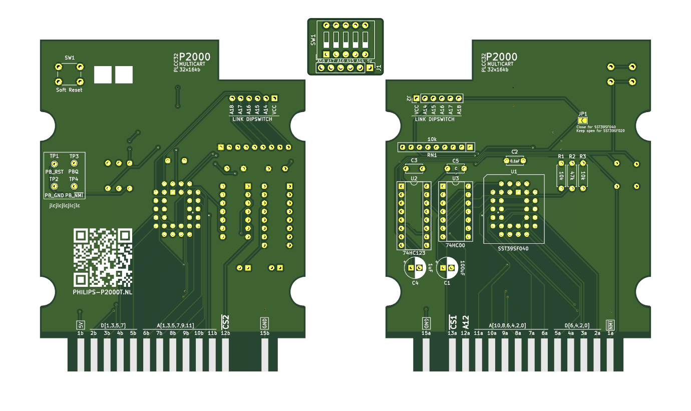
Fig. 9 Printed Circuit Board (PCB) of the multirom cartridge.#
What stands out in this design is the separate mounting plate for the DIP switch, corresponding to the small PCB in the middle. Obviously, the DIP switch could be placed on the big PCB itself. The reason for this design is to allow the DIP switch to reside on top side of the cartridge, allowing the user an easy and comfortable way to switch between the programs. A topview of the cartridge, showing the location of the DIP switch, is shown in Figure 10. This design does come at the expense of ordering two PCBs rather than one as well as some additional effort in wiring the DIP swith board to the main PCB.
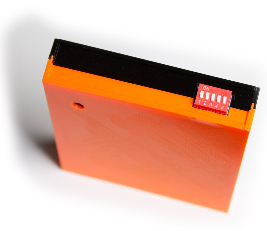
Fig. 10 Printed Circuit Board (PCB) of the multirom cartridge (top view).#
Enclosure#
In Figure 11, a render of a 3D-printable enclosure is shown. On the left, the top part of the enclosure is shown, hosting a small hole giving the user access to the soft-reset button. Both parts of the enclosure contain a small slot in which the DIP switch board is placed. The enclosure is shut tight using four M3x8mm screws. The top side of the enclosure requires four M3 threaded inserts to ensure a strong fit.
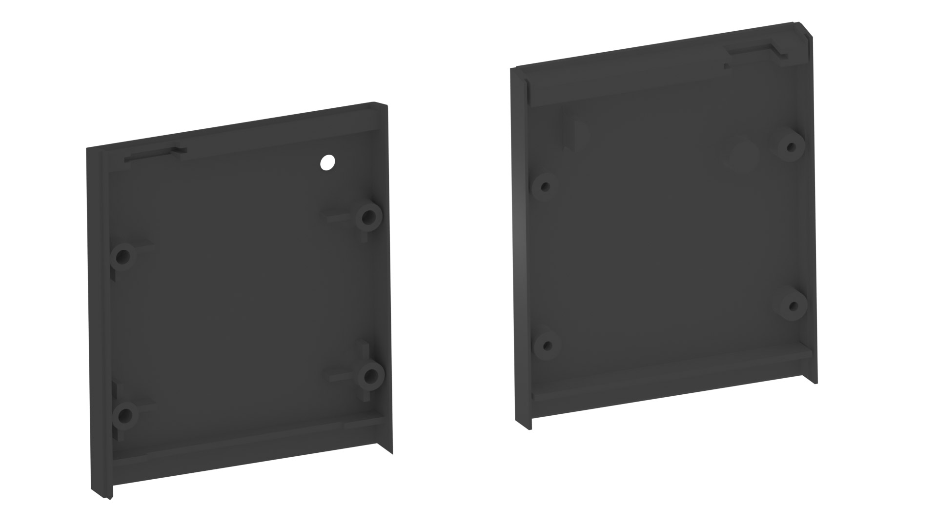
Fig. 11 3D-printable enclosure for the multicartridge.#
Cartridge roms and banking#
Assuming a SST39SF040 ROM chip is being used, the chip can host 32 different cartridge ROMs. We refer to these segments as “banks”. In other words, the ROM chip hosts 32 banks and each bank can be accessed using the DIP switch. When placing cartridge ROMs into the banks, it is important to note that a single cartridge rom may never cross a bank. Furthermore, every cartridge rom should start at the start of a bank.
The reason for this is as follows. What the cartridge essentially does is expose a 16kb bank, which corresponds to locations N*0x4000-(N+1)*0x4000 on the
ROM chip (X being a hexadecimal number in the range 0-31) to the P2000T at address 0x1000-0x5000. This segment
is fixed so no bank switching is allowed during operation and the P2000T expects a valid signatures at the start of 0x1000
so the cartridge ROM should start at the start of the bank.
Building your own multirom image, which needs to be flashed to the cartridge, is relatively straightforward. A relatively large collection of ROMs can be found on the P2000 Preservation Project. These cartridges should all be already 16kb in size. To build the multirom image, one simply concatenates these files in the desired order and store these as a new file which can then be readily flashed to the SST39SF040 chip. For the flashing, a ROM programmer is needed. Many such programmers exist at varying prices. A cheap homebrewn alternative is also presented on this website.
Source files#
All source files, i.e. the PCB design and the casing, can be found in this Github repository.