ZIF cartridge#
Introduction#
The ZIF cartridge builds upon the design of the multicartridge. The aim of this cartridge is to allow the user to easily take out the ROM chip and flash new data on it. With respect to the multicartridge that hosts a PLCC32 ROM chip inside a socket inside the enclosure, here the DIP32 variant of the ROM chip is used that is inserted in a so-called ZIF socket. The main advantage is that the user does not have to open the cartridge to take out the chip. Furthermore, the use of a ZIF socket minimizes the wear and tear on the pins of the ROM chip.
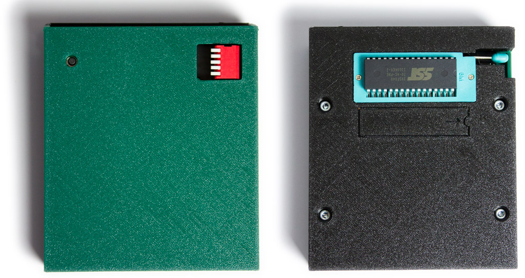
Fig. 9 Picture of the P2000T ZIF cartridge. The light blue socket on the right side of the picture is the so-called ZIF socket.#
ROM lay-out#
Similar to the multicartridge, the ZIF cartridge uses a 512kb SST39SF040 rom chip (though one could of course use one of the lower capacity rom chips). Since every SLOT1 cartridge essentially uses 16kb, this naturally divides the 512kb chip into 32 banks of 16kb. Using the piano-style DIP switch on the front of the cartridge, the user can select one of the 32 banks to load the desired cartridge.
ROM flasher#
To read and write to the SST39SF0x0 chip, a chip programmer device is required. The Xgecu TL866II is a popular choice that many electronics hobbyists use. Although this programmer supports a huge amount of chips, its price can be a bit daunting for the beginner hobbyist. There are two opportunities to save on cost. One is to develop your own programmer using e.g. a microcontroller such as the Arduino Uno or Mega. An alternative is to use the PICO SST39SF0x0 Programmer which was specifically designed to offer a low-cost programmer at the expense of only catering towards one class of rom chips (the SST39SF010, SST39SF020 and SST39SF040, either in a PLCC32 or DIP32 package).
Flashing cartridges#
A brief explanation on how to flash cartridge roms to the banks on the ZIF cartridge is provided here. This guide uses the PICO SST39SF0x0 Programmer and the flash software that is provided with this programmer. The latest version of this software can be found via the releases page of the github repository.
Note
The pictures used in this article refer to version 1.0.0 of the PICO SST39SF0x0 GUI, but the procedure remains the same.
Step 1: Opening the program#
After installing the software, you will be greeted by the screen as shown in Figure 10.
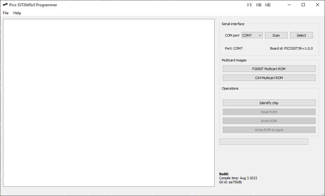
Fig. 10 PICO Flasher screen upon opening the program.#
Step 2: Loading a ROM file#
Next, open a ROM cartridge (essentially a 16kb binary file). On the left hand side, an overview of the bytes in the ROM image will be shown in hexidecimal notation. In the example provided in Figure 11, the BASICNL rom is loaded.
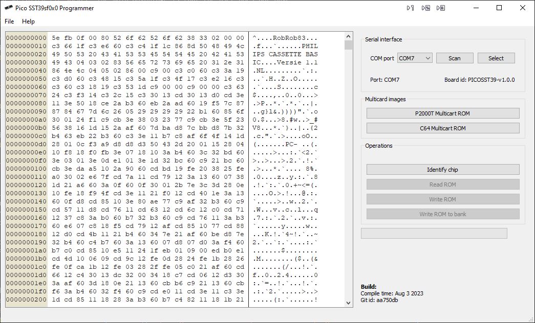
Fig. 11 PICO Flasher screen upon opening the program.#
Step 3: Connecting to the PICO flasher#
Connect to the PICO programmer by clicking on the “Scan” in the “Serial Interface” box. If the CPU
can properly interface with the flasher, it should display a board id that starts with
PICOSST39-v, followed by the version number.
Next, click on the “Identify” button to verify that your chip is indeed one corresponding to a SST39SF010, SST39SF020, or SST39SF040. The programmer essentially transmits a few instructions to the chip to get the chip id and on the basis of this id, the chip is identified.
When the chip is properly identified, click on “Write ROM to bank” and a new pop-up screen will open as shown in Figure 12. Click on the desired bank and the programmer will flash the 16kb rom to the selected bank.
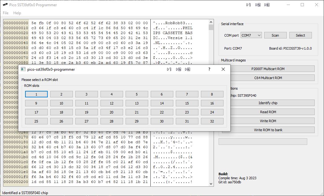
Fig. 12 PICO Flasher screen upon opening the program.#
Step 4: Writing the ROM to the bank#
The programmer will now erase the content on the bank and flash the new contents to it. After writing the new content, a verification step commences to check upon the integrity of the data. The whole process should take a bit under 20 seconds.
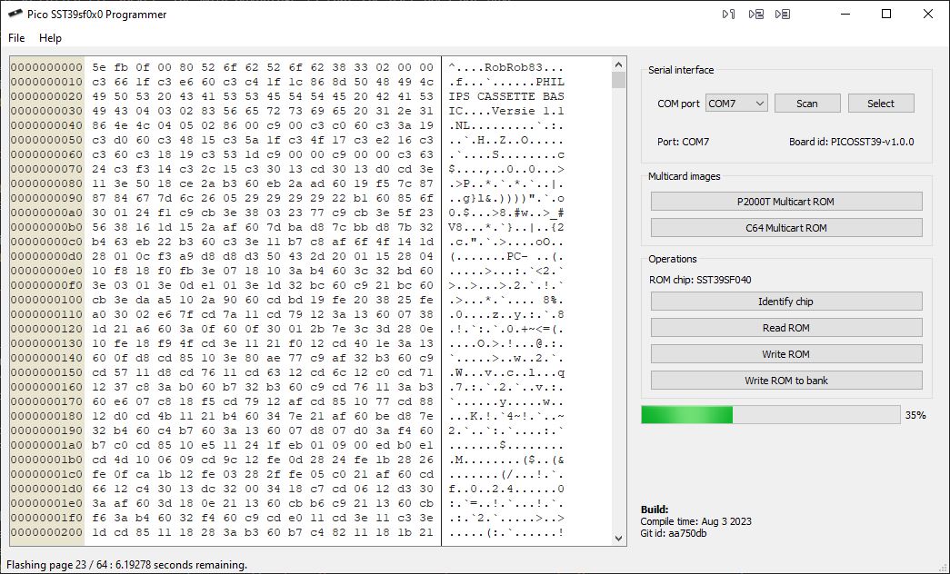
Fig. 13 PICO Flasher screen upon opening the program.#
Setting the DIP switch#
Note
If you are already familiar how binary numbers work, you can essentially skip this section and just look at Figure 14 to see which piano keys of the DIP switch correspond to which values.
In the previous section, it was explained how to flash a program to one of the banks on the ROM chip. To select the right bank on the ZIF cartridge, one need to place the keys on the piano-type DIP switch in the right position. In Figure 14, the bank address lines are indicated for each key. To illustrate the procedure, suppose we want to set the DIP switch to bank 5 (i.e. the 6th image), since 5 can be formed by (1+4), we need to depress the first and third keys from the top.
Note
We use zero-based counting the Table and explanation as shown below while the program GUI uses one-based counting when selecting the banks. In other words, the first bank is bank 0 in the Table below, but is referred to as bank 1 in the GUI.
In the Table below, one can easily look up which keys need to be depressed for each of the bank images. Note that the key positions need to be read from top to bottom. In other words, the first number (0 or 1) corresponds to the topmost keys, the second number to the key below, etc. A 0 indicates that the key should be in the upright position, a 1 indicates that the key needs to be depressed.
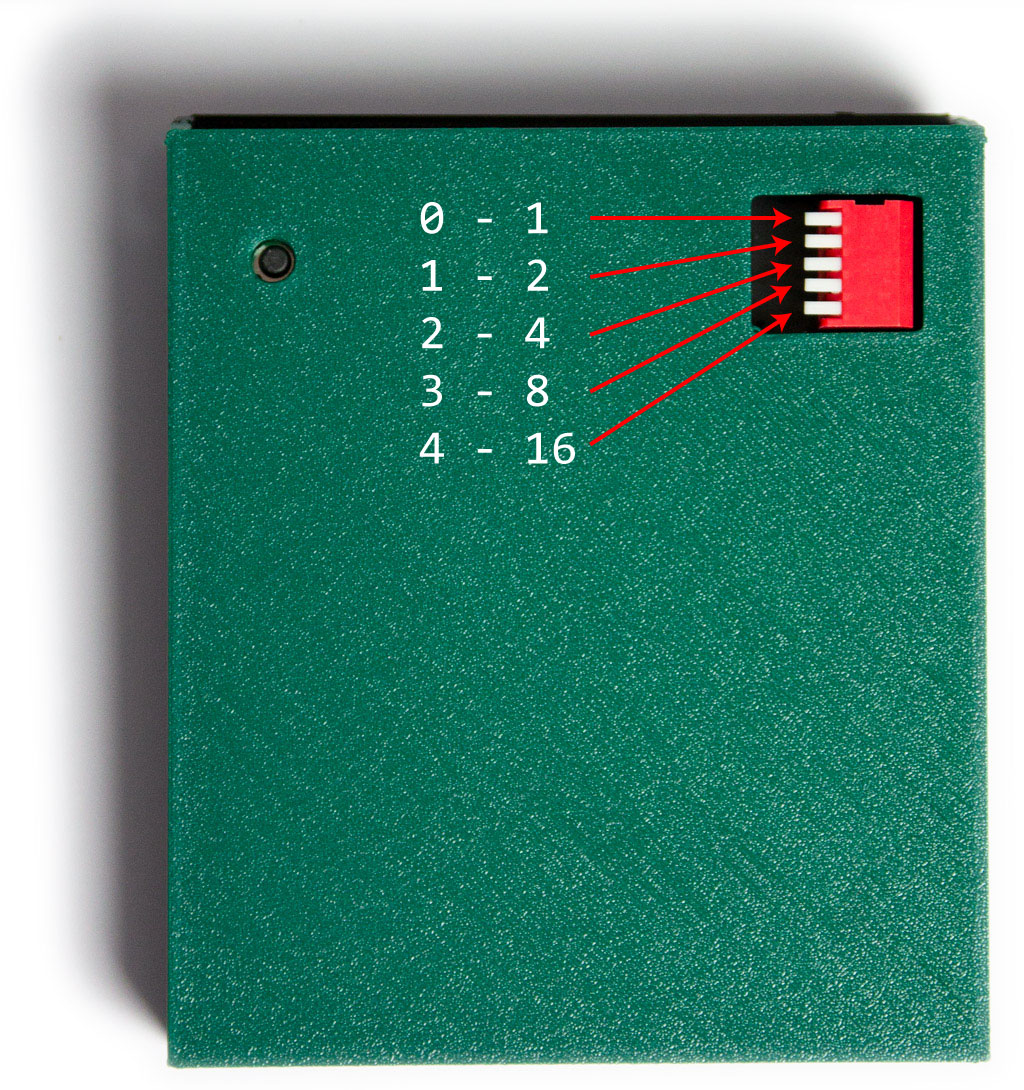
Fig. 14 DIP switch on the P2000T ZIF-cartridge.#
Table 1: Key positions for each of the banks.
| Bank number | Key positions (0=up, 1=down) | Bank number | Key positions (0=up, 1=down) |
|---|---|---|---|
| 0 | 00000 | 16 | 10000 |
| 1 | 10000 | 17 | 10001 |
| 2 | 01000 | 18 | 01001 |
| 3 | 11000 | 19 | 11001 |
| 4 | 01000 | 20 | 01001 |
| 5 | 10100 | 21 | 10101 |
| 6 | 011000 | 22 | 01101 |
| 7 | 11100 | 23 | 11101 |
| 8 | 00010 | 24 | 00011 |
| 9 | 10010 | 25 | 10011 |
| 10 | 01010 | 26 | 01011 |
| 11 | 11010 | 27 | 11011 |
| 12 | 00110 | 28 | 00111 |
| 13 | 10110 | 29 | 10111 |
| 14 | 01110 | 30 | 01110 |
| 15 | 11110 | 31 | 11111 |
Source files#
All source files, i.e. the PCB design and the casing, can be found in this Github repository.
A nice collection of homebrew programs can be found in the P2000T-programs repository.