Simple cartridge#
Tip
The source code for the PCB, the cartridge enclosure as well as the simple hello world assembly program can all be found in this Github repository.
Introduction#
The most basic cartridge that can be built for the P2000T is one wherein SLOT1
of the P2000T directly interfaces with a parallel ROM chip. The SLOT1 cartridges
essentially exposes 16kb of ROM memory accessible by the
P2000T at addresses 0x1000 - 0x4FFF. Here, it is explained in detail how such
a cartridge interfaces with the P2000T.
Note
Throughout this text, we use the notation 0x00 to refer to hexadecimal notation
of numbers.
Hardware#
The schematic for a basic SLOT1 cartridge is given below. The source files to design your own PCB can be found in the Github repository. We here explain how this cartridge works.

Fig. 1 Basic cartridge schematic.#
As can be seen from Figure 1, address pins A0-A11 directly interface
with the parallel ROM, for which in this example the relatively abundant and
cheap SST39SF010 has been chosen. The signals on pins A12 and A13 first have
to go through some logic circuitry (explained in detail below) before they
can interface with the ROM. Note that A14-A16 of the ROM are tied to
ground. Given 14 address pins (A0-A13), a total of 16kb of data is available
to the cartridge. Note that this implies that basically 112 kb of the 128 kb
total capacity of the ROM is “wasted”, though by making use of some kind of
switching circuitry (see multicartridge) we can potentially make use of the
remainder of the ROMs capacity.
The pinout of SLOT1 is documented in the Field Support Manual, under section 3.8.6 (see Figure 2). Herein, side B is the side of the PCB that is facing you when the PCB is inserted into the slot.
Caution
Observe that the pinout for pins 13A and 12B is swapped in the field manual. The correct layout is given in the schematic as shown in Figure 1.
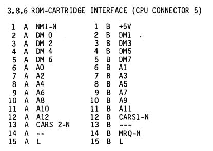
Fig. 2 Pinout of SLOT 1 as documented in the Field Support Manual. Note that pins 13A and 12B are incorrectly documented herein.#
Section 3.1 i this field manual describes the address decoding logics as
seen in Figure 3. There are two cartridge selection signals, i.e.
CARS1 and CARS2 that are active low when either the lower 8kb bank or
the upper 8kb bank of the cartridge is selected. Notably, CARS1 goes low
when A12 goes high and in a similar fashion, CARS2 goes low when A13 goes
high. In terms of interfacing with the parallel ROM, we need to introduce some
additional logic to set the right address at the ROM pins.
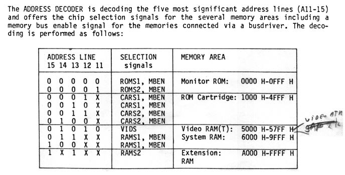
Fig. 3 Address decoding logics.#
Address line
A12of the P2000T is inverted to give address lineA12on the parallel rom chip.Line
CARS2of the P2000T is inverted to give address lineA13on the parallel ROM chip.When either
CARS1orCARS2goes low, i.e. pins 13A and 12B on the PCB respectively, theCSpin on the parallel ROM chip needs to go low as well. This is done via two NAND gates.Given the above logics, a single 74HC00 quad NAND-gate will suffice in mapping the P2000T signals to the parallel ROM.
Given the dimensions of the slot and the cartridge, i.e. the back side of a
cartridge being somewhat larger than its front side, it is recommended
when using DIP components to place them on the back side of the cartridge. A
little bit counter-intuitive is that the back side hosts the A-set of pins
whereas the front side hosts the B-set of pins. A visualization of the front
and back side of the PCB is given in Figures Figure 4 and Figure 5, respectively.
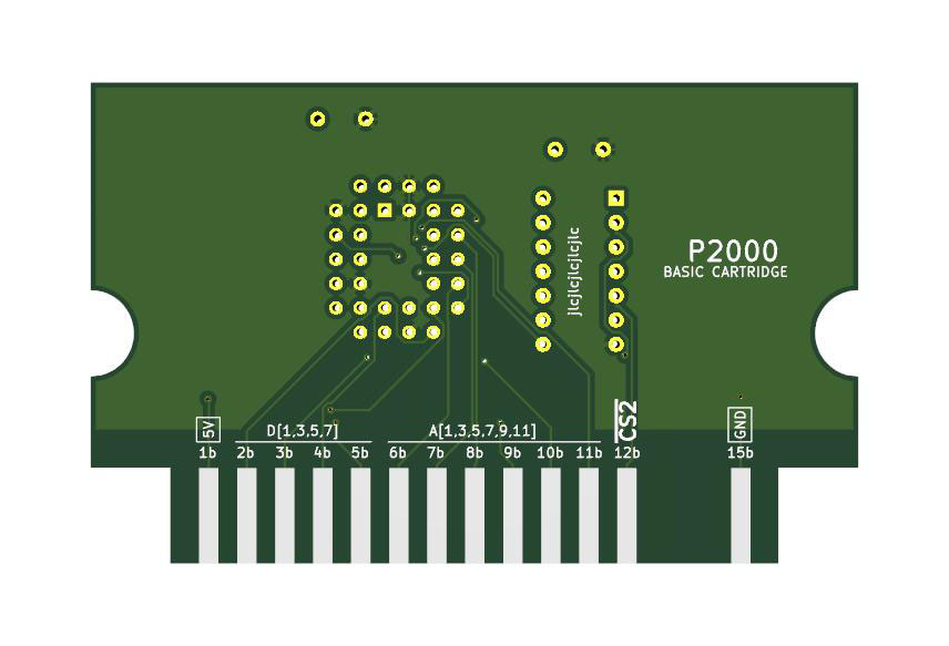
Fig. 4 Front side of the Basic Cartridge PCB. The marking jlcjlcjlcjlc is
placed on the PCB board to ask the manufacturer (here JLCPBC) to place the product
identification token at this location.#
For the SST39SF010 chip, a PLCC32 type of socket has been used. This is mainly to keep the footprint relatively small. There also exists a DIP package for this very chip, though this chip is a little bit more expensive.
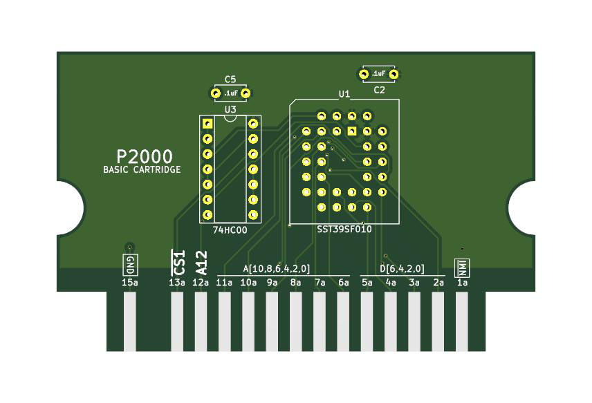
Fig. 5 Back side of the Basic Cartridge PCB.#
ROM header#
Having discussed the hardware side of the SLOT1 cartridge, we now proceed
to elaborate on the software side. The P2000T internal ROM located at
$0000-$1000 will only interface with a cartridge in SLOT1 if it contains
a certain set of valied entries in its first 16 bytes. These first 16
bytes are referred to here as the cartridge header.
The cartridge header of every ROM contain a validation byte, four byte of instructions for cartridge validation procedure and finally 11 bytes for the cartridge title, as shown in the table below.
Address |
Description |
|---|---|
|
Signature byte |
|
Number of bytes to check for checksum |
|
16 bit checksum |
|
Cartridge label |
How this cartridge is used when starting from the cartridge will be explained on the basis of a simple “hello world” program.
Simple Hello World Program#
The source code to display the display the text “Hello World” on screen,
is given in the code snippet below. The line org 0x1000 indicates that this cartridge
starts at memory location 0x1000. Next, the 16 bytes corresponding to the cartridge
header are provided as two sets of bytes. The first set contains the signature byte,
the number of bytes to be evaluated to produce the checksum and finally the 16 bit
checksum value.
The program starts with a jp printmsg instruction which copies the data at the
label message: to memory address 0x5000, which corresponds to the start of
video memory. After the data has been copied, the program is placed in an
infinite loop.
; "helloworld.asm"
; This is an example Hello World assembly file
    org 0x1000

    ; signature, byte count, checksum
    DB 0x5E,0x00,0x00,0x00,0x00

    ; name of the cartridge (11 bytes)
    DB 0x00,0x00,0x00,0x00,0x00,0x00,0x00,0x00,0x00,0x00,0x00

    ; display Hello World
    jp printmsg

message:
    DB "Hello World!",255

printmsg:
    ld hl,message
    ld bc,0x5000
print:
    ld a,(hl)
    cp 255
    jr Z,loop
    ld (bc),a
    inc hl
    inc bc
    jp print

    ; set infinite loop
loop:
    jp loop
Cartridge validation#
On start-up, any cartridge in SLOT1 is validated. The validation procedure can be understood from the disassembled monitor ROM. Starting at line 626 we observe the following code.
; check cartridge
    ld a,(Cartridge_ROM)        ; first byte of cartridge ROM
    and 0f5h                    ; mask with 0b11110101
    cp 054h                     ; egual to  0b11110100 ?
    jr nz,bootstrap             ; no cartridge signature present, try loading from tape

    ld hl,Cartridge_ROM         ; pointer to 1st byte of ROM
    ld a,(hl)                   ; get 1st byte
    bit 0,a                     ; bit 0 set?
    jr nz,bootstrap             ; then try to bootstrap

    push hl                     ; save start of cartridge
    call validate_cartridge     ; check 1st 8k bank of cartridge ROM
                                ; jumps into cassette load on checksum error
If the first byte of the ROM after and 0xF5 corresponds to 0x54 and
the first bit of the first byte is not set, then the validate_cartridge
routine is launched. In other words, if the first byte is equal to
b0001x1x1 which is 0x5E, 0x5C, 0x56, or 0x54, the validate_cartridge
routine is executed.
The validate_cartridge routine can be found on line 755 and onwards. Here, we observe that this routine is basically a 16 bit checksum based
on the arguments of the second to fifth bytes of the cartridge. The first
pair of bytes correspond to the number of bytes that need to be checked for
the checksum. The second pair of bytes corresponds to the value of the checksum.
; validate cartridge ROM
; inputs:
; HL points to 1st byte of cartridge ROM to check
; 1st 5 bytes of cartridge ROM:
; defb signature
; defw len
; defw checksum
; returns: Z flag if success
; jumps into cassette bootstrap routine on error
validate_cartridge:
    inc hl                      ; skip signature byte
    ld c,(hl)                   ; lo byte of byte count
    inc hl                      ;
    ld b,(hl)                   ; hi byte of byte count
    inc hl                      ;
    ld e,(hl)                   ; lo byte of checksum
    inc hl                      ;
    ld d,(hl)                   ; hi byte of checksum
rom_test_loop:
    ld a,b                      ; is byte count zero?
    or c                        ;
    jr nz,do_ROM_test           ; no, so keep checking
    ld a,d                      ; checksum also zero?
                                ; can be zero from the start: OK
    or e                        ; otherwise all bytes were added to DE.
                                ; result should then also be zero, if not it is a checksum error
    ret z                       ; Z is ok, NZ = checksum error
    jp bootstrap                ; try to load a program from tape

    do_ROM_test:
        inc hl                      ;get next byte
        ld a,(hl)
        add a,e                     ;add to 16 bit checksum
        jr nc,no_add_carry
        inc d                       ;handle carry
    no_add_carry:
        ld e,a                      ;sum back in e
        dec bc                      ;dec bytes done
        jr rom_test_loop
When the sum over all the bytes (as set by byte count) corresponds to the
checksum, the cartridge is validated and the cartridge launches from address
0x1010.
Cartridge enclosure#
Rather than inserting a “naked” PCB into your P2000T, it is more elegant to place the PCB inside a nice cartridge. Many electronics hobbyists now have access to 3D printers and a nice enclosure for the PCB has been designed.
The .stl files for 3d-printing an enclosure for the basic cartridge can be
found in the Github repository.
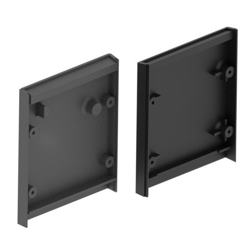
Fig. 6 Enclosure for basic cartridge. Left image is the backside and front image is the front side.#
Final remarks#
Although the “official” P2000T Field Manual contains an error in the pin lay-out for SLOT1, it is worth noting that the P2000 User Group (P2000gg; gg=Gebruikers Groep) published in one of their newsletters a nice overview page (see Figure 7) showing the pin lay-out for several of the connectors on the P2000t.
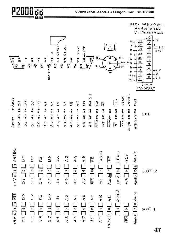
Fig. 7 Page 47 of the P2000gg 8-11 newsletter. Page obtained from: https://github.com/p2000t/documentation/blob/master/P2000gg/p2000ggnieuwsbrief8-11.pdf.#